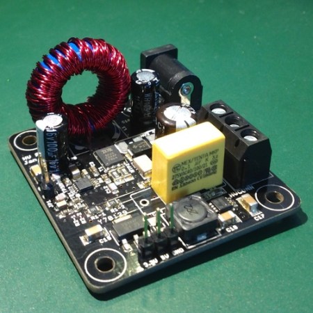
[Jan Rychter] was sick and tired of not being able to find the right power supply for his Nixie tube projects, so he decided to design his own. [Jan] started out designing around the MAX1771 (PDF) DC-DC controller, but quickly discovered he was having stability problems. Even after seven board revisions, he was still experiencing uncontrolled behavior. He ended up abandoning the MAX1171 and switching to the Texas Instruments TPS40210. After three more board designs, he finally has something that works for him. [Jan] admits that his design is likely not perfect (could have fooled us!), but he wanted to release it to the world as Open-Source Hardware to give back to the community.
The end result of [Jan’s] hard work is a 5cm x 5cm board that generates four separate output voltages from a single 12V source. These include both a 3.3V and 5V output for digital logic as well as a 220V out put for Nixie tubes and a 440V maximum output for dekatrons. The circuit also features several safety features including over-current protection, thermal shutdown, and slow-start. Be sure to check out [Jan’s] webpage to view out the schematics and technical information for this awesome circuit.
Need some Nixie tubes to go with that circuit? We know some resources for you to check out. Or you could always just build your own. How can you use this board in your next project?


well i would have done more with the HV to LV creepage spacing but thats just me
Exactly, if that was a commercial product, it would never pass the safety requirements
Haha yeah, trying not to start a debate but its not even passing FCC and UL regulations … its just plain dangerous
And every other professional EE!
Yeah i would be fired on the spot … and well deserved … if i tried to pass something like this … looks purdy tho!
Looks like it could also be tweeked and used for some of those surplus Geiger-Mueller tubes on the market. (some without mod)
You can use the little inverters for backlights to drive GM tubes. The voltage in is pretty much proportional to the voltage out.
Seems like a risky layout to me. All those exposed smd components…
definitely using this
Do you have a use in mind already?
Hi guys — author here. As for the HV trace spacing, I already got some comments on that and I’ll be improving that in a future revision. It’s less of a problem than most people think, because of the soldermask on both sides of the board, but still, I guess it’s a valid concern.
Fixing it, unfortunately, isn’t that obvious, as you need to route the feedback trace between the components somehow, and there are limits as to what you can do with tightly packed components.
I think you made an odd layout decision by placing the HV between the 12V and the 3V3/5V section. I’m going to try a different layout and let you know if it works out.
Safety in a product has much higher priority than tight space not the other way around.
Slots can be cut on PCB to increase creepage.
This page tells you what the spacing requirements are for the different voltage levels.
http://www.smps.us/pcbtracespacing.html
Well, according to the widget on that page, IPC-2221B requires 0.4mm (16mil) spacing for coated PCB traces (my case) at 220V. The current design has that spacing (or larger).
Reading the rest of the text, it seems there is no clear idea on what the spacing should be.
Remember, that there is overcurrent protection in this circuit, so the worst case isn’t as bad as in a mains-powered SMPS.
But in general, as I said — I agree, the spacing could be made larger.
As for alternate layouts, if you do manage to get a better one, please let me know — I’m very interested! It took me a lot of iterations to get to that point. Please remember about ground return currents, you do not want currents from the 5V switcher returning under the feedback trace for the HV supply. That limits your options as to placement.
Roger.
Absolute worse case if size is totally necessary and safety is not, throw a grounded guard trace around the HV part (soldermask removed and tinned) but for the love of god take the extra space and cut slots …. i have had 220v jump nearly half cm solder masked space … luckily it jumped just to ground and it simply lit the PCB on fire …
I’ve also seen that when I inspected PCBs after a year or so.
My solution is to completely seperate L & N in the layout. Have one connector for L-connections (e.g. after triacs or relays) and one connector for N-connections. As a bonus it makes routing much easier. Downside is that the wires that come in look messy.
A low-pass filter on your voltage feedback would help with your noise. As it is, the noise from the high voltage will couple directly into the output of the error amplifier through C7. A cap from the FB pin to ground would take care of it.
Peter, I disagree — C7 is part of the compensation network and is important for loop stability. Also, you definitely do not want to put a low pass filter on voltage feedback if you want good transient response.
You can move the cap one resistor up on the voltage divider to decouple from the feedback network. About the response, I’m just talking about filtering out the switching noise. Since output voltage is already a 2nd order function and there is a large output filter cap, we’re not talking about very high bandwidth to begin with.
Were you hitting a RHPZ? Very common for boost designs due to the inherent nature of the inductor current. Current-mode control is a little easier to compensate than a voltage-mode controlled converter as well.
Tossing a 0R resistor in line with the gate drive and tuning its value can help; you can usually place a 1 to 5 ohm resistor there to dampen ringing on the gate which will be magnified on the output. The combination of trace inductance and gate capacitance forms a tank that will resonate; the resistor can dampen that.
Also, using two resistors in parallel as your current-sense element make me raise an eyebrow; I would always use a single resistor, and the cost of that resistor would be factored into the design from the start. What does the error of having two resistors at the extreme edges of their tolerances get magnified into for the control loop?
Was size a major driver? A synchronous boost converter would help you from an efficiency POV and there are some very tiny dual-FET packages available. As well, the placement of your 0.1uF output capacitors could help combat noise, based on their location.
Just some quick feedback; I think it’s great you built that, documented it and put it up for all to see. Would love to discuss the design further with you if you would like. Check out Linear Tech’s application notes and datasheets; I’ve found them very helpful for SMPS design and I’ve managed to pass EMI and safety on the first try with a dozen designs at this point, mostly thanks to studying their material and other scholarly papers on the subject.
That came off a little rough I think; just want to reiterate that I loved your write-up and think it will be a great resource for others looking to learn about the subject. Wish I had the time to write up about switching design in more detail :)
Good PCB design, really? My first thought was that it could use some work… Not a knock on the original designer as it’s pretty good considering the density, but Hackaday writers should keep the opinions to themselves. Not that it’s terrible, but I wouldn’t say it’s an example to use as a gold standard by any means.
The HV portion could likely have been completely done on one side of the PCB rather than two, reducing the switching path length. Then the regulation down from the 12V could be done on the other side of the input jack rather than routing the 12V all the way across the board.
The author notes questioning if the snubber works because he only has a 100MHz scope? That’ll work fine for the job. Probing around the switching nodes will potentially answer the stability questions as well…
But, great work turning out a design that’t been iterated through, which really is the key to getting it right and learning along the way!
Ok; so this is an interesting discussion. I note the comments on safety, and those are useful. Bottom line is, though, that this is a useful project. Like the author, I have been looking for a small reproducible psu for a Nixie project, and this is the most promising so far. So thanks for all of this – both to the author/designer, and to those who made valid but focussed comments on the safety issues. I’ve learned something here.
For creapage, dust & moisture = can cause ionization failure creeping along surface for ionized arc.
Thus prudent safe layouts use an air slot cutout in board between HV and LV or a much larger gap. > 1/3″ I recall
The idea is that it might be safe with 120V but not when triggered by a 6kV transient. Then it turns into an ARC and subject connected to LV load would get jolted with voltage rise.